Japanese chipmaker Rapidus has announced the successful installation of ASML’s TWINSCAN NXE:3800E, a state-of-the-art EUV lithography machine. This system will be a critical component in Rapidus’ new IIM-1 foundry located in Chitose, Hokkaido. The delivery marks a historic milestone as it is the first time an EUV lithography tool will be used for mass production in Japan.
This development is poised to elevate Japan’s position in the global semiconductor industry, particularly in the advanced chip manufacturing domain.
The Role of the TWINSCAN NXE:3800E in Advanced Manufacturing
What is the TWINSCAN NXE:3800E?
The TWINSCAN NXE:3800E, produced by ASML, is among the most advanced extreme ultraviolet (EUV) lithography machines available today. With its ability to support high-volume manufacturing of 2nm logic nodes, it represents a significant leap forward in semiconductor production capabilities.
ASML remains the sole global supplier of EUV photolithography equipment, critical for manufacturing cutting-edge chips at 3nm, 5nm, and now 2nm scales. The system uses a 0.33 numerical aperture (NA), ensuring precise and efficient chip fabrication.
Complementary Equipment for Optimal Performance
In addition to the TWINSCAN NXE:3800E, Rapidus plans to install a suite of advanced semiconductor manufacturing tools and fully automated material handling systems. These upgrades aim to optimize the production process for 2nm generation gate-all-around (GAA) semiconductors.
IIM-1 Foundry: A Hub for Innovation in Hokkaido
Construction and Milestones
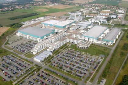
Rapidus’ Innovative Integration for Manufacturing (IIM-1) foundry is under active construction in Chitose, Hokkaido. This facility is designed to house cutting-edge technology that aligns with Japan’s goal of becoming a leader in semiconductor manufacturing. A pilot production line is scheduled to begin operations in April 2025, laying the groundwork for high-volume production.
Introducing Rapid and Unified Manufacturing Service (RUMS)
The company is also developing a novel semiconductor foundry model called Rapid and Unified Manufacturing Service (RUMS). This service will leverage single-wafer processing for all manufacturing equipment, ensuring agility and efficiency in chip production.
Implications for Japan’s Semiconductor Industry
The installation of ASML’s lithography machine is a pivotal step for Japan, which has historically been dependent on international semiconductor production. Rapidus’ investment in cutting-edge infrastructure and equipment demonstrates its commitment to revitalizing the domestic chipmaking sector and contributing to global supply chain stability.
Frequently Asked Questions (FAQ)
1. What is EUV lithography, and why is it important?
EUV lithography is a technology used to etch intricate patterns onto semiconductor wafers, enabling the production of advanced chips. It is essential for creating smaller, more efficient, and more powerful semiconductors.
2. Why is the TWINSCAN NXE:3800E significant?
This ASML machine is the only EUV lithography system capable of supporting high-volume manufacturing at 2nm logic nodes, making it critical for next-generation semiconductor production.
3. When will the IIM-1 foundry begin operations?
The pilot production line at the IIM-1 foundry is expected to be operational by April 2025.
4. What is Rapidus’ RUMS initiative?
RUMS, or Rapid and Unified Manufacturing Service, is a new semiconductor foundry service model that emphasizes flexibility and efficiency using single-wafer processing technology.
5. How does this development impact Japan’s semiconductor industry?
The installation of advanced equipment like the TWINSCAN NXE:3800E positions Japan as a competitive player in the global semiconductor market, boosting domestic production capabilities.


